
Environmentally Friendly
Printed Electronics
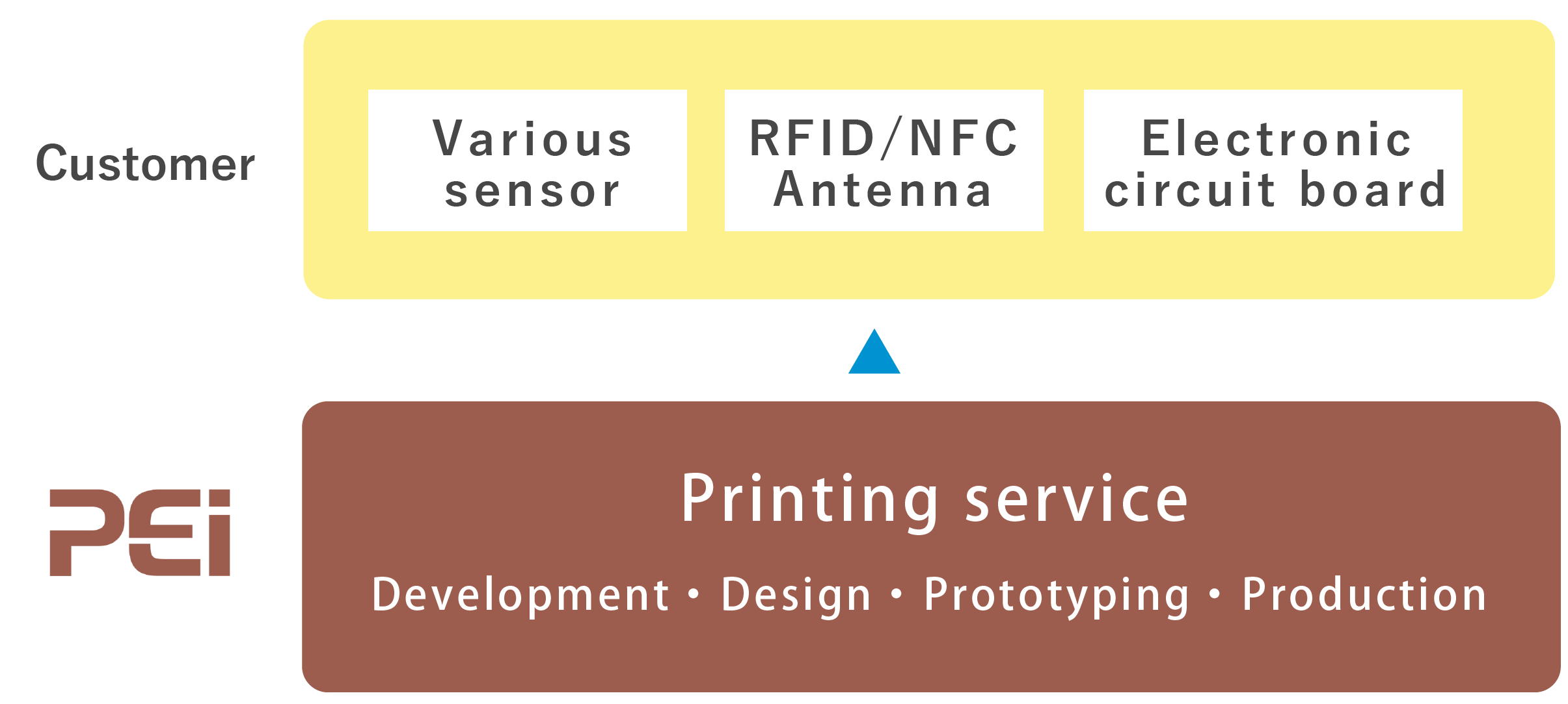
Antenna and Circuitry
Environmentally Friendly
Printed Electronics
Antenna and Circuitry


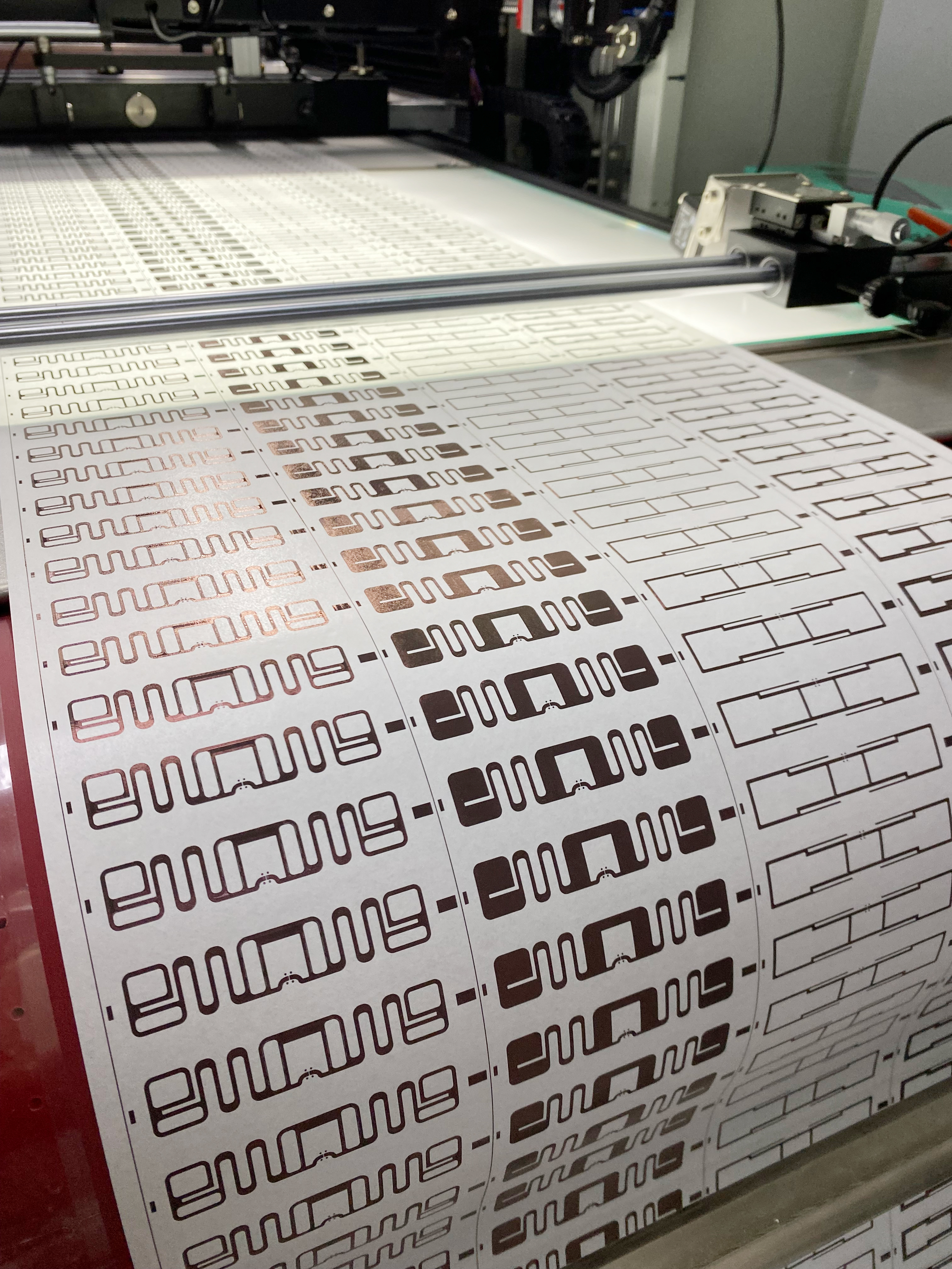
PE Innovation Co., Ltd. deliver environmentally friendly printed antenna and circuitry using Perfect DRY™ process with nano Cu ink. Recently no pollution by exhaust and waste water in production process is challenged and attracted attention to avoid global warming and abnormal weather.
PE Innovation Co., Ltd. provides printed electronics technology using the Perfect DRY™ production method, which does not use any water, chemicals, or special gases, and realize contributes to the development of a sustainable society.

Printing Electronics Technology using nano-copper ink is perfectly environmentally friendly and excellent cost-effective.

Due to the impact of global warming and abnormal weather, new approaches are required to prevent pollution from exhaust and wastewater during the antenna and circuitry manufacturing process. Current conventional circuit board manufacturing uses large amounts of water and electricity, along with chemicals, increasing concerns about its impact on the environment.
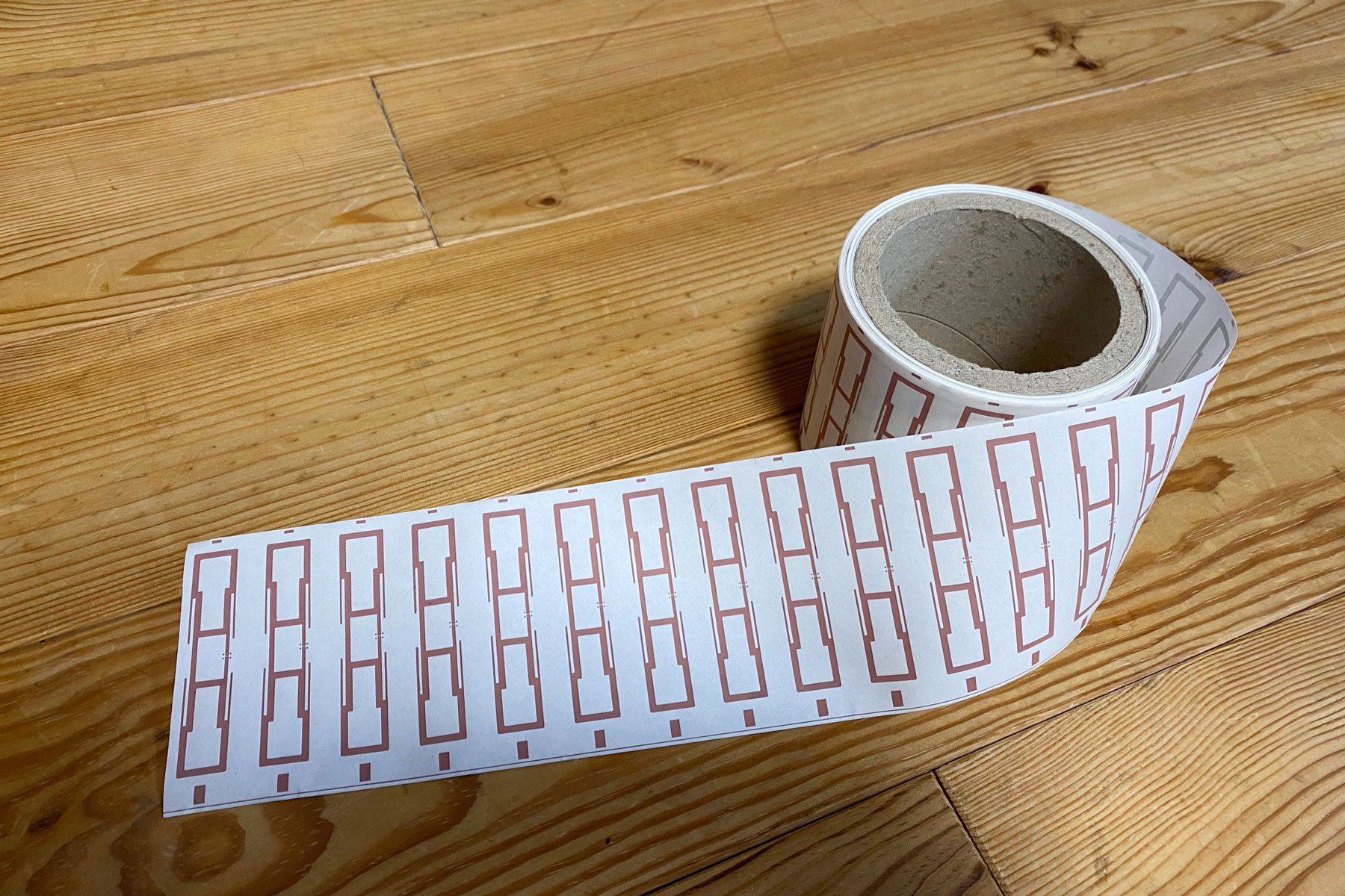
The Perfect DRY® production method provided by PE Innovation Co., Ltd. significantly reduces the environmental impact. The copper used as raw material is 100% recycled. FR4, polyimide, PET, and other printing substrates can be selected as before, using plant-based paper makes it possible to create environmentally friendly products.
Until now, printed electronics has normally used silver ink. However, due to spike of recent price of silver,
the price difference between silver and copper in terms of raw material costs is more than 200% (based on the market prices of silver and copper, as of December 2025).
In terms of conductivity, which is a key characteristic, nano-copper ink has the same properties as silver ink, achieving high cost performance.
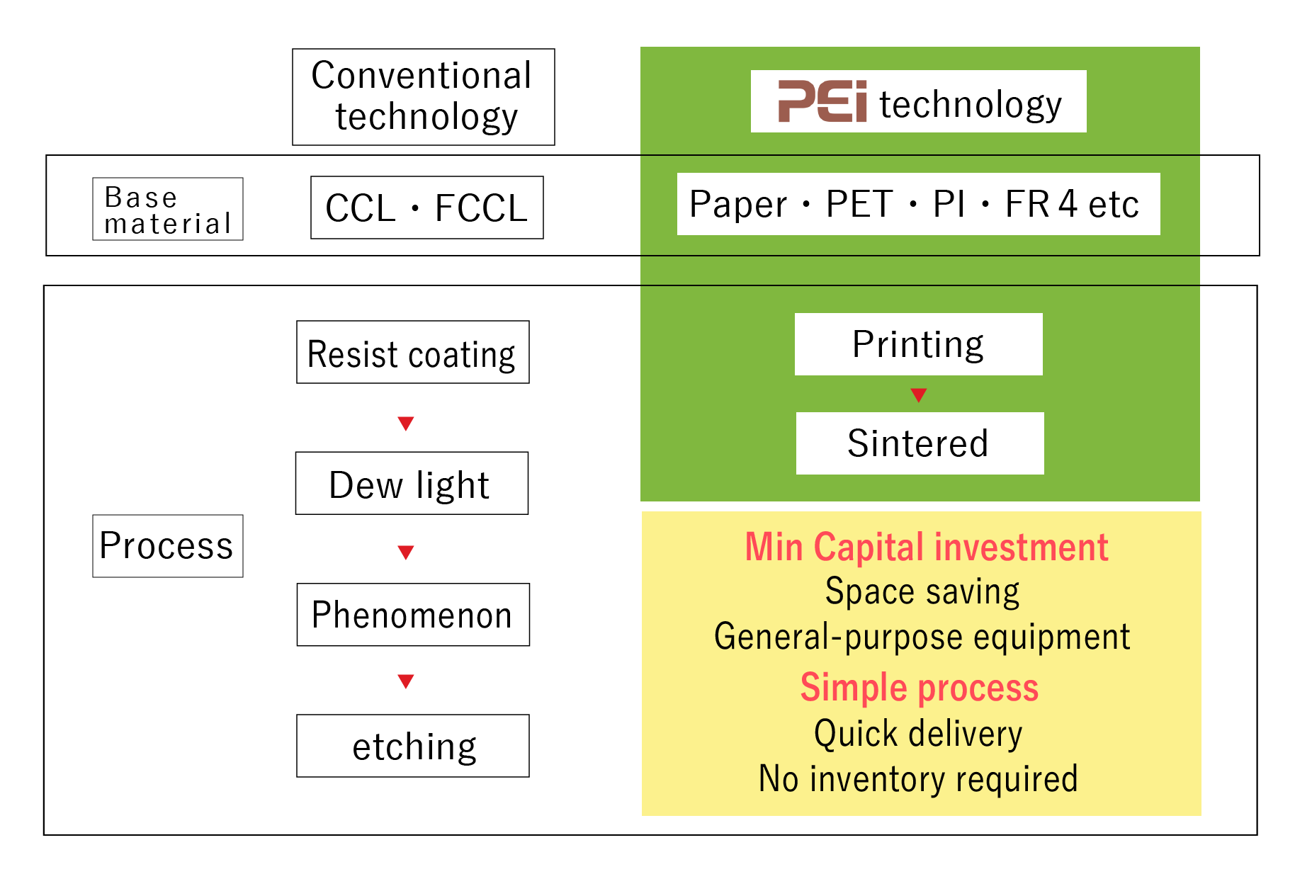
The circuitry formation technology provided by PE Innovation Co., Ltd. is a quite simple production process consisting of printing, drying, and sintering. The production process uses the Perfect DRY® method, which does not use special gases or chemicals, and allows for sintering in a flash time without pressure or in an atmospheric atmosphere.
Because the production process is simple, it saves production space, capital investment and is highly productive, allowing for short delivery lead times.

PE Innovation Co., Ltd. is collaborating with Tatsuta Electric Wire Co., Ltd.,
a manufacturer of nano copper ink, to provide antenna and circuitry printing services.

| Company Name | PE Innovation Co., Ltd. |
| Location |
HQ Hashimoto Building 501, 5-4-5 Asakusabashi, Taito-ku, Tokyo 111-0053 Kyoto PE Center 3-17 Osadanomachi, Fukuchiyama City, Kyoto 620-0853 Tokyo R&D Center Shirahige Nishi R&D Center 303, 8-5-7 Minamisenjyu, Arakawa-ku, Tokyo 111-0003 |
| Establishment | September 12, 2024 |
| Capital | 25,000,000 JPY |
| Main bank | Resona Bank Ueno Branch |
| Co-founder |
President CEO Mike Sakaguchi Director CTO Masayuki Orihashi Director COO Akito Nishimura |